Stop struggling with messy breadboards that fall apart every time you sneeze. Designing a custom PCB at home is now simpler and more affordable than ever, with free software tools and manufacturing services that produce professional-quality boards for less than your morning coffee run. You can go from circuit idea to working board in just one week using tools available to anyone with a computer and internet connection. This guide cuts through the confusion to show you exactly how to design PCB at home without wasting money on failed prototypes or getting overwhelmed by complex software.
Choose the Right PCB Design Software for Your First Project

Why KiCad Beats Free Alternatives for Beginners
KiCad isn’t just free—it’s the industry standard for hobbyists creating professional-quality boards from home. Install it on Windows, Mac, or Linux and immediately access features that rival $10,000 commercial tools. The initial learning curve seems steep, but most beginners complete their first functional board within 48 hours of focused learning. Critical advantage: KiCad generates manufacturer-ready Gerber files without limitations or watermarks, unlike many “free” alternatives that restrict output quality.
Don’t waste time with these common mistakes:
– Avoid building custom footprints for your first board
– Skip complex 3D modeling until you master 2D layout
– Ignore advanced features like impedance control initially
EasyEDA for Browser-Based Design Beginners
If installing software feels intimidating, EasyEDA runs directly in your browser with zero setup time. The integrated JLCPCB ordering system lets you go from design to manufacturing in minutes. Perfect for absolute beginners, EasyEDA’s visual interface makes component placement intuitive. Pro tip: Use EasyEDA to learn core concepts, then migrate to KiCad for more complex projects as your skills grow.
Create Your First Circuit Diagram That Actually Works
Why Sourcing Proven Designs Beats Original Designs
Your first PCB should replicate a working circuit—not invent something new. Start with these beginner-friendly projects that guarantee success:
– Blinking LED circuit (5 components total)
– 555 timer LED flasher (8 components with clear functionality)
– Simple voltage regulator (3 components with visible output)
Source reliable designs from:
– GitHub repositories with active communities
– Hackaday projects with documented builds
– Open-source hardware sites like SparkFun
The Critical Component Check Most Beginners Skip
Over 70% of first-time PCB failures stem from incorrect component specifications. Before finalizing your design:
– Verify transistor pinouts—TO-92 packages vary by manufacturer
– Confirm LED voltage drops—blue LEDs require different resistors than red
– Check capacitor polarity markings—reversed electrolytics cause instant failure
Pro tip: Print your board layout at 1:1 scale and physically place components on the paper to verify footprints before ordering.
Design Your PCB Layout Without Costly Mistakes
Through-Hole Component Placement That Works
Position components strategically for both electrical performance and physical assembly:
– Place inputs on left, outputs on right to follow natural signal flow
– Keep related components together—position timing resistors near your 555 timer
– Leave 5mm clearance around board edges for easy handling
Critical mechanical considerations:
– Avoid placing tall components near connectors
– Ensure USB ports align with enclosure cutouts
– Position heat-generating parts near board edges
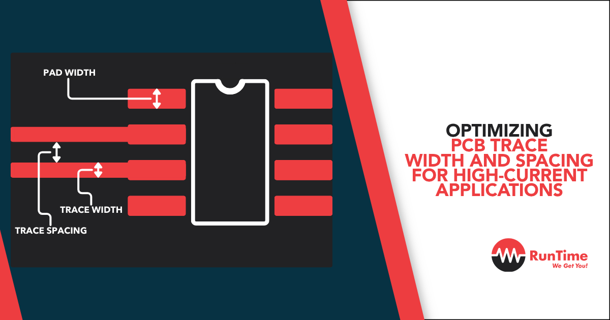
Trace Routing Rules for First-Time Success
Follow these conservative guidelines for your first PCB design at home:
– Power traces: Minimum 1.0mm (40 mil) width
– Signal traces: 0.5mm (20 mil) standard
– Clearance: 0.5mm (20 mil) between all traces
– Via size: 1.0mm diameter with 0.5mm hole
Routing sequence that prevents errors:
1. Connect ground pins to ground plane first
2. Route power supply traces (VCC, +5V)
3. Wire critical signal paths
4. Complete remaining connections
5. Run Design Rule Check (DRC) before finalizing
Generate Manufacturing Files That Won’t Get Rejected
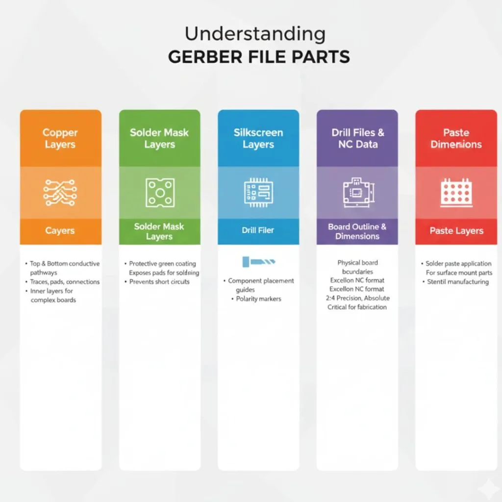
The Gerber File Checklist Before Ordering
Manufacturers reject 30% of first-time orders due to incomplete file packages. Generate these essential files:
– Copper layers (Top and Bottom)
– Solder mask (Top and Bottom)
– Silkscreen (component labels)
– Drill file (exact hole locations)
– Edge cuts (board outline)
Verification steps:
– Open files in Gerbv Gerber viewer
– Check for missing copper areas
– Verify board outline matches dimensions
– Confirm component labels are visible
JLCPCB vs. OSHPark: Which Service Saves Beginners Money?
For your first PCB design at home, these services deliver the best value:
– JLCPCB: $2 for 10 boards (100×100mm max), $20 DHL shipping
– OSHPark: $5 per square inch with distinctive purple soldermask
Cost-saving strategies:
– Design within 100×100mm for cheapest pricing
– Order 5-10 boards minimum for base price
– Panelize multiple small designs on one board
Assemble Your PCB Without Damaging Components
Essential Tools for Home PCB Assembly
Skip expensive equipment and start with these basics:
– Temperature-controlled soldering iron (set to 350°C)
– Fine tip (0.5mm for precision work)
– 0.6mm 60/40 rosin-core solder wire
– Flux pen for stubborn joints
– Magnifying glass for inspection
Workspace setup tips:
– Sort components by value using labeled containers
– Print component placement diagram
– Use helping hands or PCB holder
– Ensure bright, direct lighting
Step-by-Step Assembly Sequence for Fewer Mistakes
Follow this order to minimize assembly errors:
1. Solder small components first (resistors, diodes)
2. Add integrated circuits (use sockets for easy replacement)
3. Install connectors and switches
4. Solder larger components (capacitors, inductors)
5. Final assembly (heatsinks, mechanical parts)
Quality checkpoints:
– Check for solder bridges between pins
– Verify all components sit flush with board
– Confirm polarized components orientation
– Clean flux residue with isopropyl alcohol
Test Your Board Before You Get Discouraged
Systematic Power-Up Procedure for New PCBs
Power your board safely with this sequence:
1. Visual inspection for shorts and cold joints
2. Resistance check between power and ground
3. Gradual voltage increase while monitoring current
4. Functional testing of each circuit section
Essential tools:
– Multimeter for voltage and continuity checks
– Current-limited power supply
– Bright LED for quick status indication
Fix These 3 Common First-Board Problems
Problem: Board doesn’t power up
Solutions:
– Check for reversed power supply polarity
– Verify component orientation (ICs, diodes, capacitors)
– Measure for short circuits between power rails
Problem: Intermittent operation
Solutions:
– Resolder suspicious joints
– Add decoupling capacitors near ICs
– Check for cold solder joints under magnification
Plan Your Next PCB Design to Level Up Skills
From Single-Layer to Double-Sided Boards
Once your first board works, advance your PCB design at home skills:
– Level 1: Single-sided boards with through-hole components
– Level 2: Double-sided boards with 1206 SMD components
– Level 3: Four-layer boards with impedance control
Transition strategy:
– Start with 1206 size SMD components
– Use hot air rework station for easier assembly
– Design stencils for consistent solder application
Your first custom PCB might seem intimidating, but thousands of hobbyists successfully create working boards every week. Start with a simple LED flasher circuit, order from JLCPCB, and you’ll hold your professionally manufactured circuit board within two weeks. The skills you develop designing PCBs at home open doors to creating custom Arduino shields, IoT devices, or even commercial products. Remember—every expert was once a beginner who ordered their first board and learned from any mistakes. Your journey to professional-quality PCB design starts with that first click of the “order” button.